CÔNG TY TNHH MLAB
  • Tìm kiếm nhiều:
  • AI Computer
  • Raspberry Pi
  • NVIDIA Jetson
  • Máy tính nhúng
  • Màn hình LCD ....

Danh mục

    OpenEP4CE6-C Package B, ALTERA Development Board
    OpenEP4CE6-C Package B, ALTERA Development Board
    OpenEP4CE6-C Package B, ALTERA Development Board
    OpenEP4CE6-C Package B, ALTERA Development Board
    OpenEP4CE6-C Package B, ALTERA Development Board
    OpenEP4CE6-C Package B, ALTERA Development Board
    OpenEP4CE6-C Package B, ALTERA Development Board
    OpenEP4CE6-C Package B, ALTERA Development Board
    OpenEP4CE6-C Package B, ALTERA Development Board

    OpenEP4CE6-C Package B, ALTERA Development Board

    3,398,000VNDLiên hệ

    Sản phẩm nhập khẩu chính hãng Waveshare

    Hỗ trợ kỹ thuật trong suốt quá trình sử dụng

    Xuất hóa đơn GTGT cho cá nhân, đơn vị có nhu cầu

    Sản phẩm được bảo hành 06 tháng


    Thông tin sản phẩm

    OpenEP4CE6-C Package B, ALTERA Development Board

    FPGA Development Board Designed For ALTERA Cyclone IV Series, Features The EP4CE6 Onboard, And Integrates Various Standard Interfaces, Pretty Easy For Peripheral Expansions.

    EP4CE6 development board

    Overview

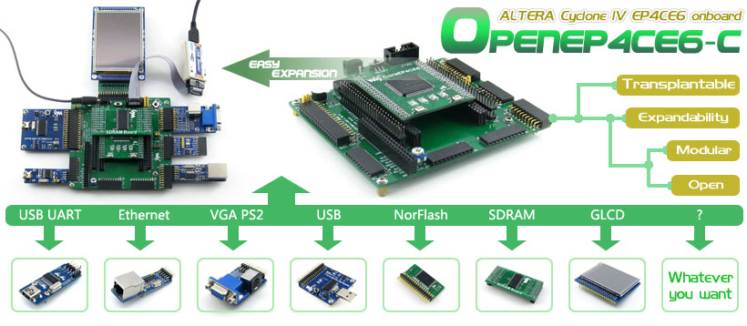
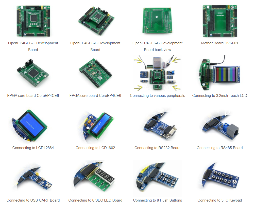
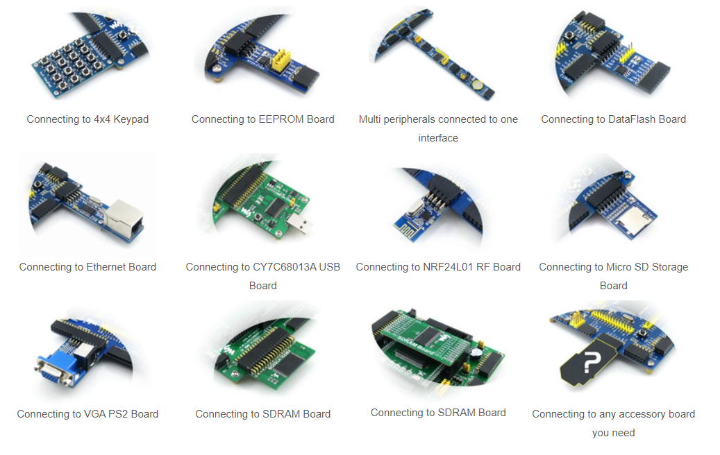
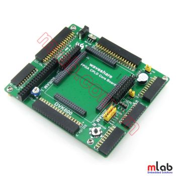
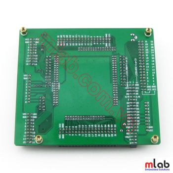
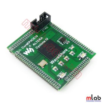
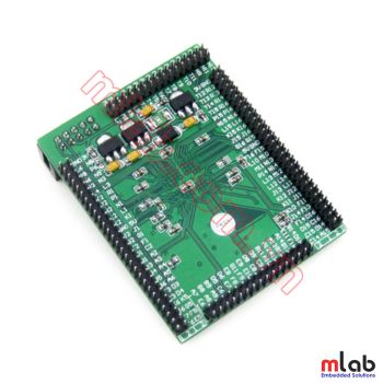
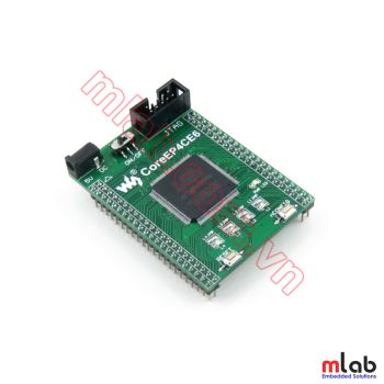
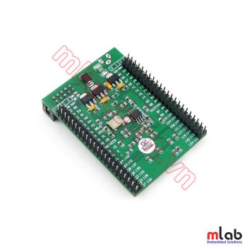
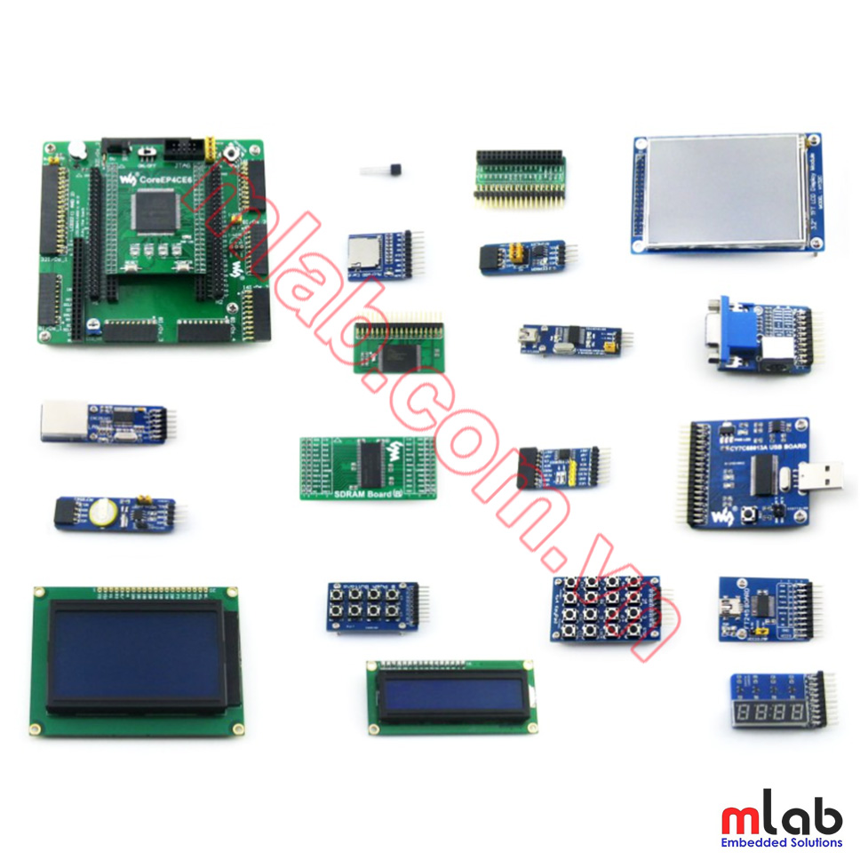
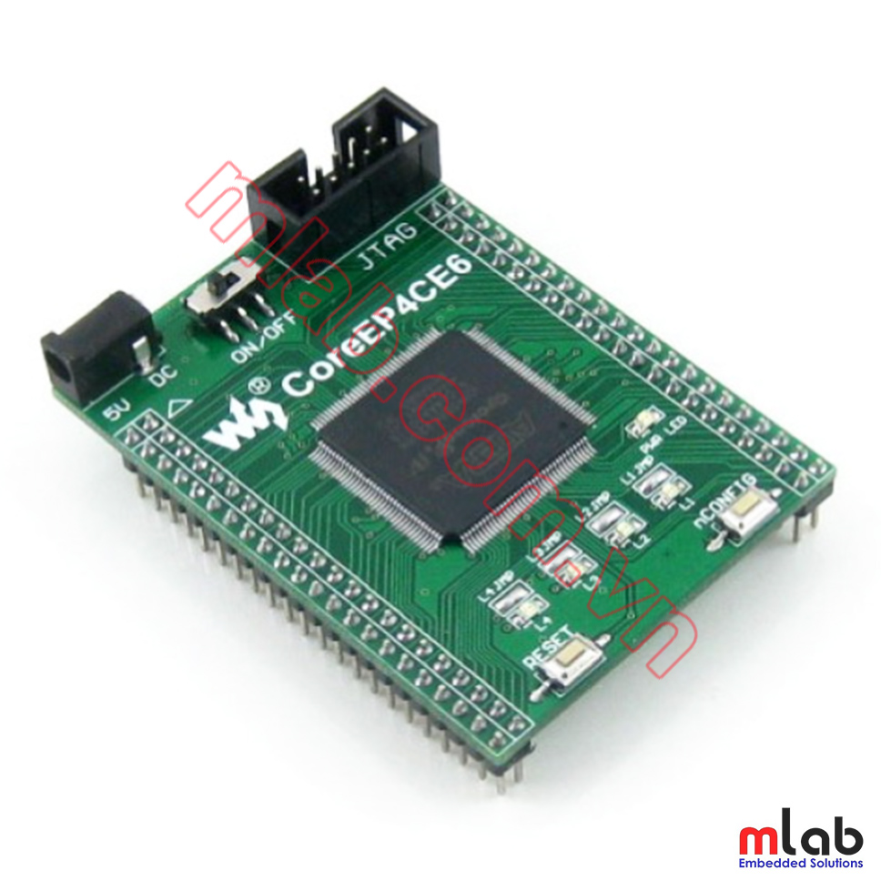
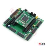
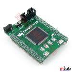
    OpenEP4CE6-C is an FPGA development board that consists of the mother board DVK601 and the FPGA core board CoreEP4CE6.

    OpenEP4CE6-C supports further expansion with various optional accessory boards for specific application. The modular and open design makes it the ideal for starting application development with ALTERA Cyclone IV series FPGA devices. OpenEP4CE6-C enables you to start your design with the Nios II processor easily and quickly.


    What's on the mother board

    FPGA CPLD development board on board resource

      1. FPGA CPLD core board connector: for easily connecting core boards which integrate an FPGA CPLD chip onboard
      2. 8I/Os_1 interface, for connecting accessory boards/modules
      3. 8I/Os_2 interface, for connecting accessory boards/modules
      4. 8I/Os_3 interface, for connecting accessory boards/modules
      5. 8I/Os_4 interface, for connecting accessory boards/modules
      6. 16I/Os_1 interface, for connecting accessory boards/modules
      7. 16I/Os_2 interface, for connecting accessory boards/modules
      8. 32I/Os_1 interface, for connecting accessory boards/modules
      9. 32I/Os_2 interface, for connecting accessory boards/modules

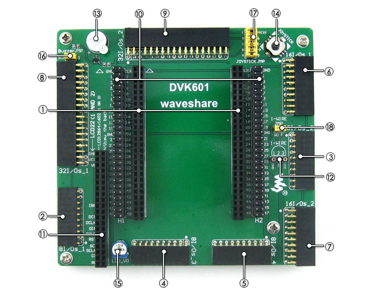
    All the I/O interfaces above:

        • capable of being simulated as USART, I2C, SPI, PS/2, etc.
        • capable of driving devices such as FRAM, FLASH, USB, Ethernet, etc.
      1. FPGA expansion connectors
        • FPGA pins are accessible on expansion connectors
        • for connecting SDRAM accessory board
      2. LCD interface, for connecting LCD22, LCD12864, LCD1602
      3. ONE-WIRE interface: easily connects to ONE-WIRE devices (TO-92 package), such as temperature sensor (DS18B20), electronic registration number (DS2401), etc.
      4. Buzzer
      5. Joystick: five positions
      6. Potentiometer: for LCD22 backlight adjustment, or LCD12864, LCD1602 contrast adjustment
      7. Buzzer jumper
      8. Joystick jumper
      9. ONE-WIRE jumper

    For jumpers 16-18:

      • short the jumper to connect to I/Os used in example code
      • open the jumper to connect to other custom pins via jumper wires

    The DVK601 supports a wide range of different core boards, therefore, some of the interfaces may be Not-Connected and useless while connecting to certain core board. For instance, while connecting to Core3S250E, the '④ 8I/Os_3' and '⑤ 8I/Os_4' are Not-Connected.


    What's on the CoreEP4CE6

    EP4CE6E22C8N core board on board resource

      1. EP4CE6E22C8N:the ALTERA Cyclone IV FPGA device which features:
        • Operating Frequency: 50MHz
        • Operating Voltage: 1.15V~3.465V
        • Package: QFP144
        • I/Os: 80
        • LEs: 6K
        • RAM: 270kb
        • PLLs: 2
        • Debugging/Programming: supports JTAG
      2. AMS1117-3.3, 3.3V voltage regulator
      3. AMS1117-2.5, 2.5V voltage regulator
      4. AMS1117-1.2, 1.2V voltage regulator
      5. EPCS16, onboard serial FLASH memory, for storing code
      6. Power indicator
      7. LEDs
      8. Reset button
      9. nCONFIG button: for re-configuring the FPGA chip, the equivalent of power reseting
      10. Power switch
      11. 50M active crystal oscillator
      12. 5V DC jack
      13. JTAG interface: for debugging/programming
      14. FPGA pins expander, VCC, GND and all the I/O ports are accessible on expansion connectors for further expansion
      15. LED jumpers

    Photos


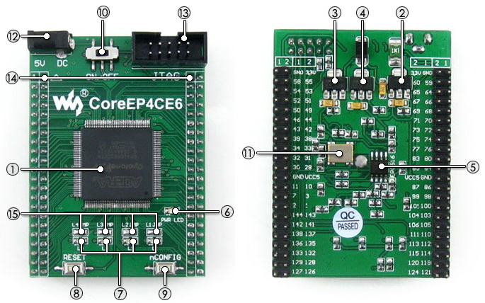
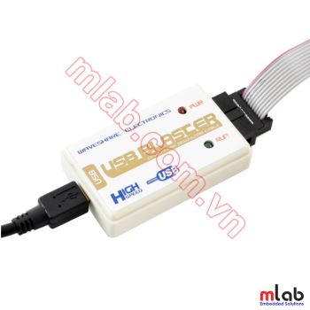
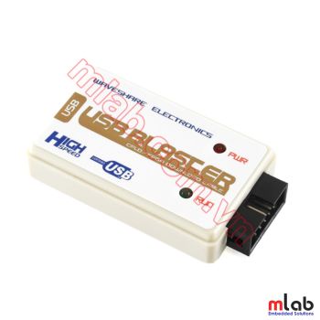
    Note: The OpenEP4CE6-C does NOT integrate any programming/debugging function, a programmer/debugger is required.


    Examples

    The OpenEP4CE6-C FPGA development board comes with various examples codes for the supported peripherals, which give you a quick start to develop your own application.

    PERIPHERAL DESCRIPTION INTERFACE VERILOG VHDL NIOS II C
    S29GL128P NorFLASH 32I/Os     Y
    AT24CXX EEPROM I2C
    FM24CXX FRAM I2C
    AT45DBXX DATAFLASH SPI    
    SD card FLASH SPI    
    H57V1262GTR SDRAM parallel    
    PCF8563 RTC I2C    
    DS18B20 Temperature sensor 1-WIRE
    SP3232 Serial communication UART
    SP3485 Serial communication UART
    PL2303 USB TO UART UART
    FT245 USB TO FIFO parallel    
    CY7C68013A USB DEVICE I/Os    
    ENC28J60 Ethernet controller SPI    
    Buzzer Sound device 1I/O (PWM)
    PS/2 keyboard Input device PS/2  
    Single buttons Input device ----
    4x4 keypad Input device 8I/Os
    Joystick Input device 5I/Os
    LED Display device ----
    8 SEG LED Display device 13I/Os
    VGA monitor Display device VGA  
    Character LCD Display device 11I/Os  
    Graphic LCD Display device 11I/Os    
    3.2 inch multi-color LCD + touch screen Display device + Input device 32I/Os    

    Debugging/Programming Interface

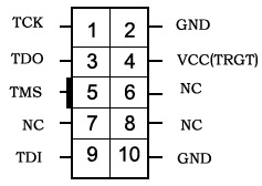
    The OpenEP4CE6-C FPGA development board integrates JTAG interface for programming/debugging.

    JTAG Signal Names & Description

    PIN SIGNAL NAME DESCRIPTION
    1 TCK Clock signal
    2 GND Signal ground
    3 TDO Data from device
    4 VCC(TRGT) Target power supply
    5 TMS JTAG state machine control
    6 NC No connect
    7 NC No connect
    8 NC No connect
    9 TDI Data to device
    10 GND Signal ground

    JTAG Header Pinout

    10-pin JTAG header pinout


    Development Resources

      • Related Software (Quaters II, NIOS II etc.)
      • Demo Code (Verilog, VHDL and NIOS II C)
      • Schematic (PDF)
      • FPGA Development Documentations (Datasheets etc.)

    Wiki: www.waveshare.com/wiki/OpenEP4CE6-C


    Khách hàng đánh giá
    5.0
    5
    0%
    4
    0%
    3
    0%
    2
    0%
    1
    0%

    Chia sẻ nhận xét về sản phẩm

    Đánh giá và nhận xét

    Gửi nhận xét của bạn

        Bình luận
        Gửi bình luận
        Bình luận

          Sản phẩm liên quan

          Đặt hàng trước
          DVK600 Mạch mở rộng cho FGPA/CPLD
          DVK600 Mạch mở rộng cho FGPA/CPLD
          Đặt hàng trước
          CoreEP4CE10 FPGA Altera Cyclone IV
          CoreEP4CE10 FPGA Altera Cyclone IV
          Đặt hàng trước
          DVK601 Mạch mở rộng cho FPGA/CPLD
          DVK601 Mạch mở rộng cho FPGA/CPLD
          Đặt hàng trước
          CoreEP4CE6 FPGA Altera Cyclone IV
          CoreEP4CE6 FPGA Altera Cyclone IV